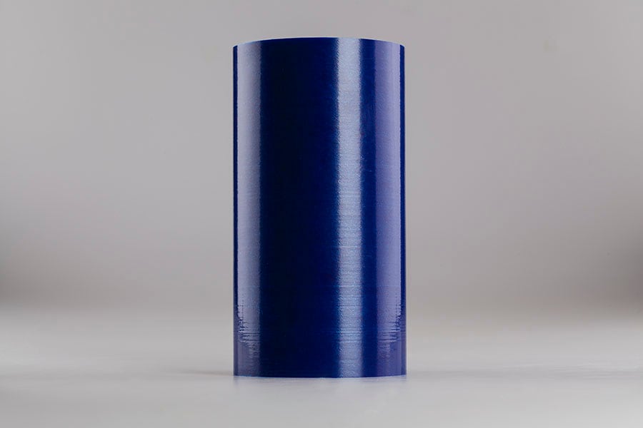
Semiconductor Wafer Processing Tape SWT 10T+R
Wafer processing tape designed for semiconductor dicing processes.
Nitto Semiconductor Wafer Tape SWT 10T+R is designed for semiconductor dicing processes. This product consists of a clear transparent PVC film coated with a pressure sensitive acrylicbased adhesive manufactured in clean room environment. For easy unwind, the backing of the PVC-film is coated with a silicone release. The product is wound on a plastic core. Rolls are individually packed in a double polyethylene anti-static bag and foreseen with lot number.
Features
- Excellent deformation behaviour, even with thicker base film
- Excellent adhesion level
- Easy unwind
- Recyclable
- Clean room product
- REACH compliant
Structure
- Pressure sensitive acrylic-based adhesive
- Clear transparent PVC film (better visual inspection)
- Silicone release coating
Properties
| Film type | Plasticized PVC Film | |
| Adhesive type | Acrylic-based | |
| Total thickness | 0.130 mm | EN 1942 |
| Carrier thickness | 0.120 mm | |
| Adhesive thickness | 0.010 mm | |
| Adhesion to Si-wafer | 120 cN/20 mm | JIS Z 0237* |
| Unwind force | 60 cN/20 mm | EN 1944 |
| Tensile strength MD | 90 N/20 mm | EN 14410 |
| Elongation MD | 270 % | EN 14410 |
| Ionic Impurities | < 3 ppm | Ion Chromatography Analysis** |
| Colour | Transparent | |
| Transport and storage conditions | Temperature 15 to 30°C | |
| Relative humidity 40 to 75% RH |
*Measured on CZ-N Polished Wafer 4 inch (100) 2.5-3.5 (Shinethu Handoutai co.). Peel-off angle 90°.
**(Na+, K+, Cl-, NO2-, NO3-, PO43-, SO42-).
CAUTION: The above are typical values and should not be used in writing specifications.
Details from the test methods are described on the customer product specification.
Application
Nitto Semiconductor Wafer Tape SWT 10T+R is an ideal product for processing semiconductor wafers, to be applied on the backside of the wafer (non-active side).